Battery pack build

OK. Wow. This is going a lot slower than expected. Very detailed work, double, triple, quadruple checking. So much effort. Took me about 2 hours to get 2 cell groups together, and a tab for one end, and balance lead between the 2 groups. A lot harder doing this as a stick, with short nickel strips so they don’t stick out. And lots of kaptan tape. Such great stuff!

So break for the night, pick it up tomorrow. Don’t want to make any mistakes.

And currently being halfway done, the length is just about what I estimated originally the battery length would be. Yippee! That’s pretty great. Worst case looks like a few mm over.

1 Like

That’s a good description of custom battery pack building, yup. There’s a reason most of the commercial packs are laid out the way they are, and it’s mostly “Ease of building” reasons. There’s a lot you can do that works, but, as you’re learning, is just tedious to build.

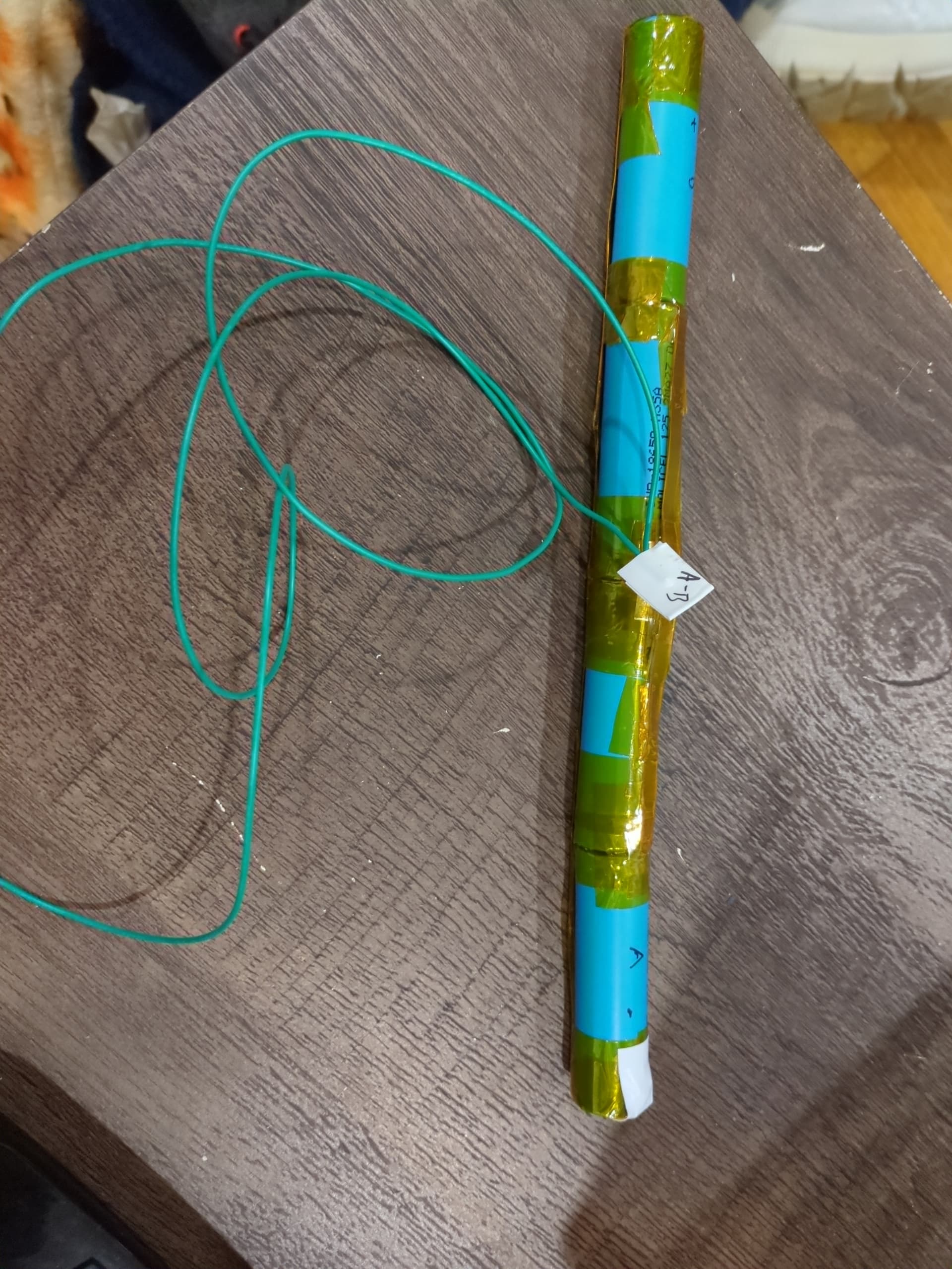
I have a battery stick!

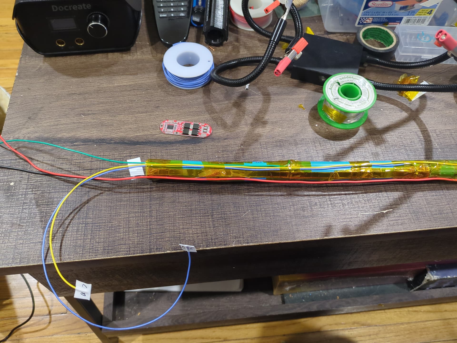
So the wires are way longer than they need to be. Way longer. Considering that I don’t have finalized 3D prints to hold the BMS and rest of the bits, I’m OK with that.
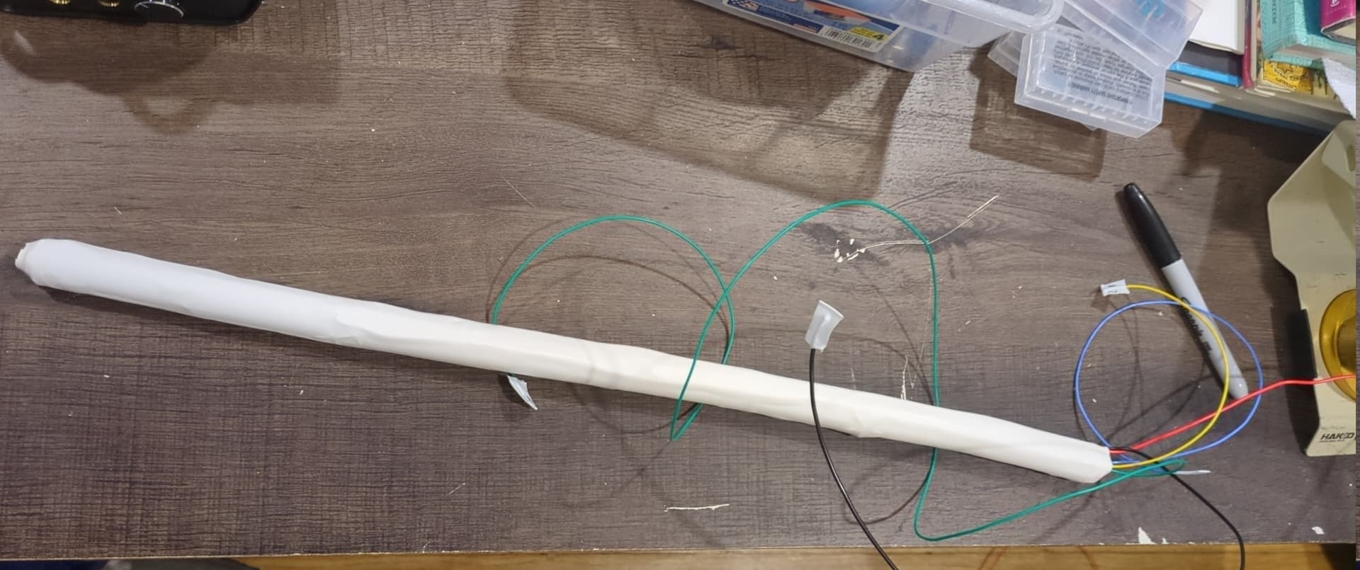
Added a small bit of stick on foam on the top and bottom, in case there’s some vertical impact, to give it a bit of cushion. Makes it a bit longer, as does the heatshrink. Although I probably can trim a touch of that off. Still works out to just about what I expected, within a few millimeters, which is pretty great.

And unfortunately it’s going to be raining for the next few days, so my intention to print in ABS and acetone finish to increase the edges of the layer bonding can’t be done, since that should be done outside.

So in short, it’s progressing. I did do a quick test print in PLA of a part fitting around the stick to keep it centered, but looks like I’m going to need to make a whole bunch of individual custom fit/designed bits, because of the varying wiring and nickel strips between parts.

All the wires are labeled, which 2 cell groups are on either side of it, so it’ll be easy to match up to the right BMS location. And I checked the Pos and Neg ends, reads something like 12.3-12.4v. Right about what it should for 4 cell groups, with the cells being a touch over 3v each before starting assembly.

The 2nd 2 cell groups went a lot faster, with experience gained with the first pair.

I think v3 (or v2.5) I’m actually going to do up a PCB and get it printed with various MOSFET controls, and bucks for each LED strip, separate LDO/buck for the ESP32, that sort of thing. Probably get the length down a LOT. Speaking of which, I’m probably going to need to remove a lot of the vertical inter-part height on my current prototype pieces. I think I’ve left too much room for most of them. Slightly easier to put together is nice, but I think I actually need to claw back some centimeters of height in order to fit it all. Plus I need to do some kind of bottom foot. Contemplating getting a few bits of nice hardwood, different colors, and use my router to give them some turned wood look, somehow, something more than just a straight round that fits over top of the bottom of the cane as a foot. Hm, some rock maple might be sturdy enough to be used. Or maybe one of these swivel feet from McMaster. Decisions decisions…


Better a foot longer than a quarter inch short! :slight_smile:

Does this surprise you? Anything like this is a learning/optimization experience, and you get faster as you go. Custom work is always slow until you learn how to do it better. I definitely got faster at the big BionX battery packs I was building over time - I’d build 4-5 of them in parallel, finishing all of one type of step before moving on.

I like that big self-leveling foot, though… that would probably work very well!

Yeah, I though that foot seemed good. I’m not questioning it though…there’s not a whole lot of room going to be left inside the bottom for a bolt insert to attach it well. Although I might be able to gain another cm or bit more, I can go back to the plastics shop and ask them to chop off the handle which inserts into the cane.

I don’t want to increase the height much, although I do suppose another cm or two will be OK.

EDIT: Hm. Not sure if the ball joint is what I want. It’s not too expensive, so maybe I’ll try it, but a flat sorta feels more like a cane. Plus, it’ll be more predictable. Hmm

So…you know those little castleated edges of an ESP32? Well…soldering on to them and expecting it to stay through manipulation might have been a little optimistic.

So I made a small carrier board I can solder the ESP32 I have already, with through-holes to solder the wiring to. I think it’ll be fairly easy to solder it down to, and should be juuuust narrow enough to squeeze in. Next batch probably will end up being with a small SMT LDO that can take in a wider range of voltages, and ESP already mounted. If I ever need more like this, beyond what I already have.

Here’s the github GitHub - Drizzt321/ESP32-pinout-carrier: An ESP32 board to bring out the pins on the module to easy to solder through-hole. Can manage up to 22awg wiring.

Apparently someone has already found this and forked it. Hopefully I didn’t steer them wrong, and it won’t quite fit. shrug I guess I’ll find out next week.

Oh. Yeah. Those half-through vias are good for:

(1) Mounting to a set of 0.1" headers sticking up.
(2) Soldering directly to something else’s plated through hole vias.

That’s about it. :slight_smile:

Didn’t think about soldering 0.1" headers onto it. If I cut them down, should be enough space to fit it then, and then solder to the post.

However, the PCBs have shipped. Unfortunately, they’re scheduled for this Thur sometime. Not as fast as I was hoping. Oh well. I’ll have enough time, so I’ll just wait for my boards. But using some of the 0.1" headers is a good fallback, if I end up having issues with the PCBs and need to just get it done.

Yeah, stuff the header rows in a proto board or breadboard or something, and make a structural solder joint. That way, you’ve got the pin “plastic holder thing” helping share load too. I’d make a somewhat larger-than-required solder joint for that use as well - and then you should be fine. Just be careful that you don’t melt that connection out while you’re soldering wires on.

But hopefully the breakout board works well!

Well blast. So the pads are spaced just a tiny fraction a bit farther apart than is ideal. Perhaps 0.5-1mm. Oh well. I managed to form a solder bridge far across it.

But unfortunately, they seem to not be booting up sigh Or at least, it’s not creating the “no WiFi settings, so open up an Access Point”. And those headers…the castleated is I think ~0.05" spacing, not 0.1" spacing. Still got some of those on, just soldered to about every-other pin. Still nothing. Even when I connect to a separate test/serial/breakout board for bare modules, which has 0.1" header pins, and I use those for 3.3v & GND from USB 5v.

But when I remove the module and put it back on the test/breakout module, it generates an AP. Although it seems to take a bit of extra time doing so.

Could I be damaging the modules with the heat from the soldering?

EDIT: And while the LDO is outputting 3.3v, I am seeing that the spec sheet says Vin only to 12v.Which currently it’s at…but it won’t end up being. So I need to redo the buck for the ESP32

And…while this was sitting here for quite a while, a random search and a bit more reading revealed, probably to nobody else’s surprise, the EN pin needed a 10K pull-up resistor to 3.3v facepalm

Worked like a charm on the board after that sigh

sigh Another screw up. Apparently I bought the 3S selection on the BMS, not the 4S. Although they are identical looking boards to the 5S. Same A, B1, B2, B3, B+, B- pads. Must be why it’s not charging, ugh.

Found what appears to be the same board on Amazon, but labeled as a 4S board in the description & title. So guess what I’m doing tomorrow night? Every so carefully un-taping, un-glueing, and desoldering everything on the BMS. And everything is cut perfectly to size…so this is going to be an interesting exercise getting it apart without cutting down the wiring any further.

Yeah, a 4S pack on a 3S board would register as overvoltage.

Quite a few of the BMS ICs are flexible like that - wire them up and you can configure them as quite a few different pack sizes. Board should be labeled with what it actually is, though.

So on Amazon found what appears to be the exact same board I bought, but for 4s. And someone commented that they can just change the 3s/4s/5s with just a jumper. Looking at the pictures on Amazon (but not Aliexpress of course…) it shows some 0 ohm resistors and open pads in a certain order.

Looking at the Aliexpress listing which has the 3s/4s/5s wiring images, and I see that each image has a different configuration of 4 SMD pads at one end of the PCB. Hm. Looks like I might be able to just remove some 0 ohm resistors, and do a small solder bridge, and it’ll work. No documentation on it at all of course.

Unfortunately, it’s going to be hell to extract/rotate it enough to get at that part of the board. Probably will have to unsolder one or two bits. Definitely at least the Neg in, which will be easy, and electrical tape over it to be sure it won’t short with anything.

That’s consistent with my knowledge of various BMS chips. Good luck!

Well, that was a PITA. And thought there was a real problem, had to take off the kaptan tape I had managed to get it into place perfectly sigh Ah well. Just have to put it back into place again. Had to kickstart the BMS with some charging, seemed to think it was too low so wasn’t outputting enough power. Give it a few watt-hours, and now up to ~13v overall, and powers up the buck converters. Yay!

EDIT: And re-wired a bit more, because I realized I need to pull out the GND for each of the LED strips, and the buck for the ESP32 was hugely annoying and not going to be easy to work with, so rewired that section too. But nearly there! Time for bed now. And I realized there’s going to be some kind of really annoying issue when I go to glue the 3D printed pieces together, holding them in place with enough force so the surfaces are together, and aligned for the LED strips.

I really need to start working on a single main integration board that carries pretty much all the bits. Even if the bucks are simply set on top and soldered onto it via through-hole and with a dab of glue to keep them in place. Just run all the “wiring” through traces on the board, and simple PCB through hole header spots so I can easily get the wiring pulled off for the LED strips. And have a basic simple LDO already onboard for the ESP32, and add in an appropriate voltage divider to measure the battery once I figured out the right values. And a small LED to show basic power on to the ESP32. And provide an easy “BMS in” and “charging in” and “connect 3-way switch here” to provide all the main controls. Wire management would be SO much simpler, and I wouldn’t hardly have to do any finicky soldering because I have very little to solder while any boards or anything are next to/on the 3D printed parts and the wires are very short.

Seems like this is really a v0.8 or v0.9 for the new cane.

Batteries sure are fun, aren’t they? :wink:

Heh, sometimes.

Ended up somehow frying the ESP32, so had to program a new one and put it onto the carrier board, and then add the resistor to the EN. Went faster and better. I’ve been getting practice (for better or worse…). Got it all wired in, powers from the battery, controls the LED and triggers the EN on the 5v bucks and turns them off when the LEDs are turned off, so the quiescent current won’t exist.Decided last minute to add UART Tx-Rx leads in advance, juuuust in case. Not sure I’ll terminate them to anything, just tape the ends off and curl them up.

I swear, I am SO going to make a larger PCB with all the bits and bobs carried through traces, and with nice header points to more easily plug/unplug/solder things and not have a bajillion wires and tight spaces to solder and squeeze and push things into.